Works
We support in "creating the future"
We support the evolution of digital devices working in the background.
Fasford Technology develops, designs and manufactures semiconductor manufacturing equipment as well as offering sales and services.
A manufacturing process of semiconductors is separated into "front-end process", which covers from designing a schematic diagram of a semiconductor to building circuits on a wafer, and "back-end process", which covers from wafer dicing to completion of a semiconductor product including assembly and final inspection.
Fasford Technology's strong field is die bonder equipment, which is used in the die bonding process in the back-end process. Our product development capability, advanced technology and customer service are highly recognized by semiconductor makers around the world and excellent manufacturing contractors for back-end process, and we hold a high market share in the global industry.
What is "die bonding"?
"Die bonding" is the process of attaching a cut out die to a substrate for packaging.
After wafer dicing, only good quality dies are selected, mounted on package die pads and then secured with adhesives, etc.
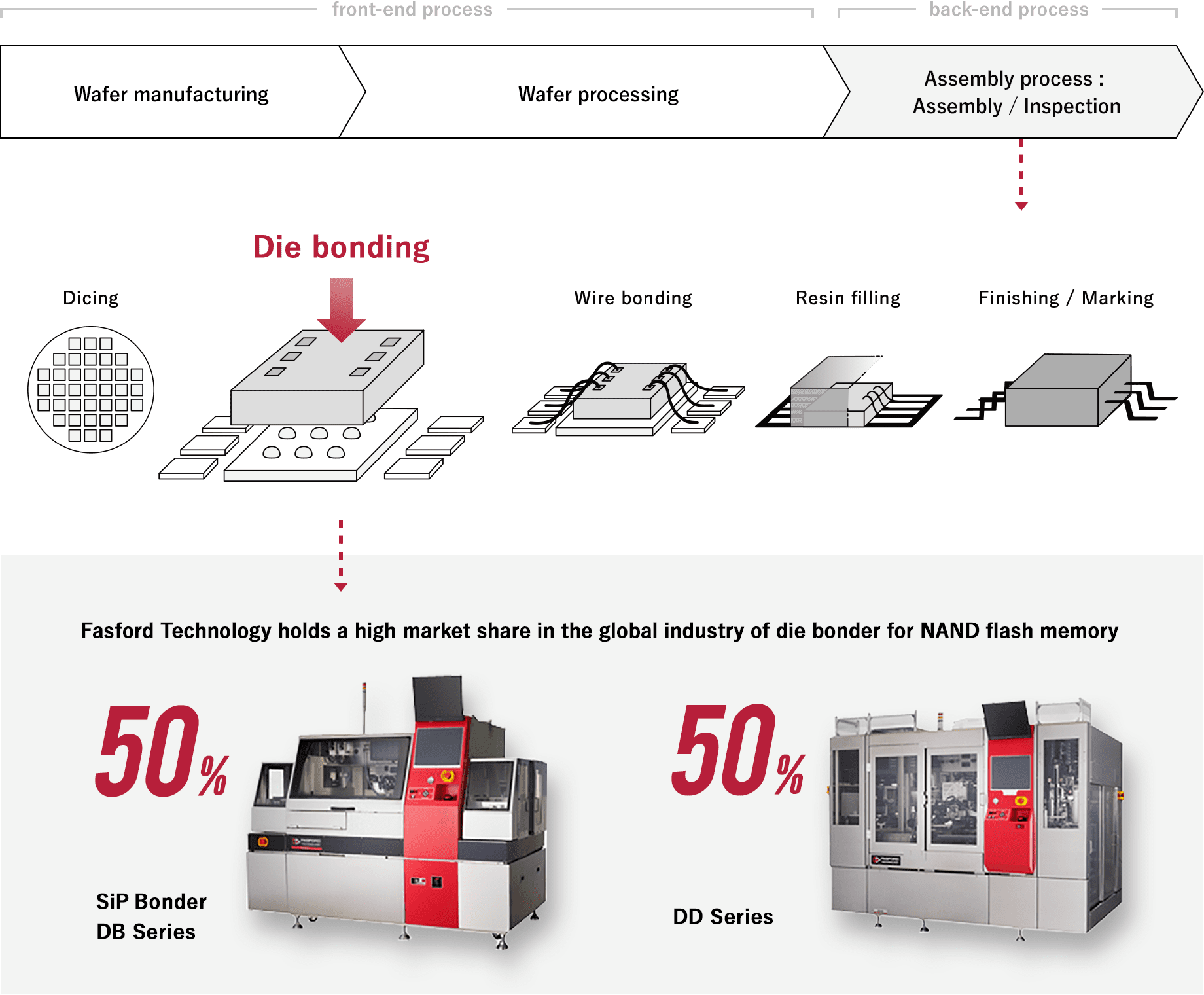
Today, the structure which stacks up to 16 layers of dies of 25μm in thickness is mass-produced and even thinner dies and increase in the number of its layers are desired in future. It is also Fasford Technology's strength to be able to provide technology to stack those thin dies accurately without damaging them.