Message
Our philosophy is to challenge and grow together with our customers and partners, with SPEED as our motto.
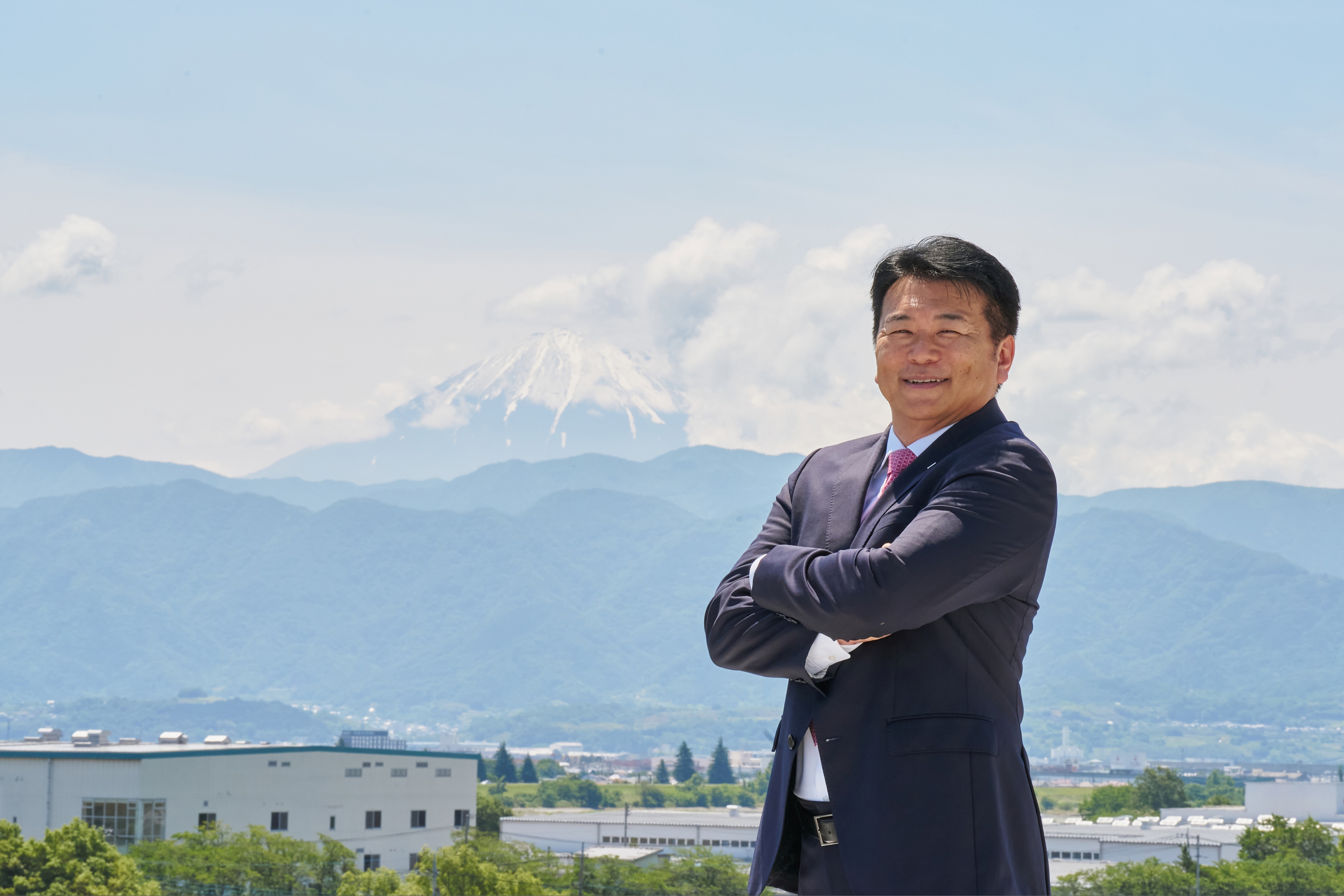
I am Hiroyuki Ao, the newly appointed President and CEO of Fasford Technology Co., Ltd.
I would like to express my sincere gratitude for your continued support and partnership.
For many years, we have been dedicated to the development of die bonding equipment for semiconductor manufacturing.
Die bonders are devices that pick up IC chips from wafers and mount or stack them onto lead frames or package substrates. Fasford Technology was the first company in the world to develop die bonding equipment capable of handling 12-inch wafers. We continue to maintain a strong market share, especially in the field of stacked die bonding for memory devices used in SSDs and the main memory of smartphones.
Our achievements are supported by proprietary advanced technologies, including high-precision die stacking at designated positions and the ability to handle ultra-thin wafers—just 25 to 40 microns thick, comparable to a plastic convenience store bag—without causing damage, thanks to our low-stress techniques. These innovations embody our commitment to exceptional precision and quality.
As semiconductor technology evolves rapidly, our vision of “Leading the world with bonding technology” requires us to respond swiftly to market changes, continuously refine cutting-edge bonding technologies, and embrace challenges with SPEED.
Through advancing the development of semiconductor back-end process equipment, we aim to contribute to the global availability of high-quality electronic devices and to enrich the lives of people around the world. We remain committed to leading the global market with our bonding technologies and achieving further growth.
We sincerely ask for your continued support and encouragement as we embark on this new chapter.
President & CEO
Fasford Technology Co., Ltd.